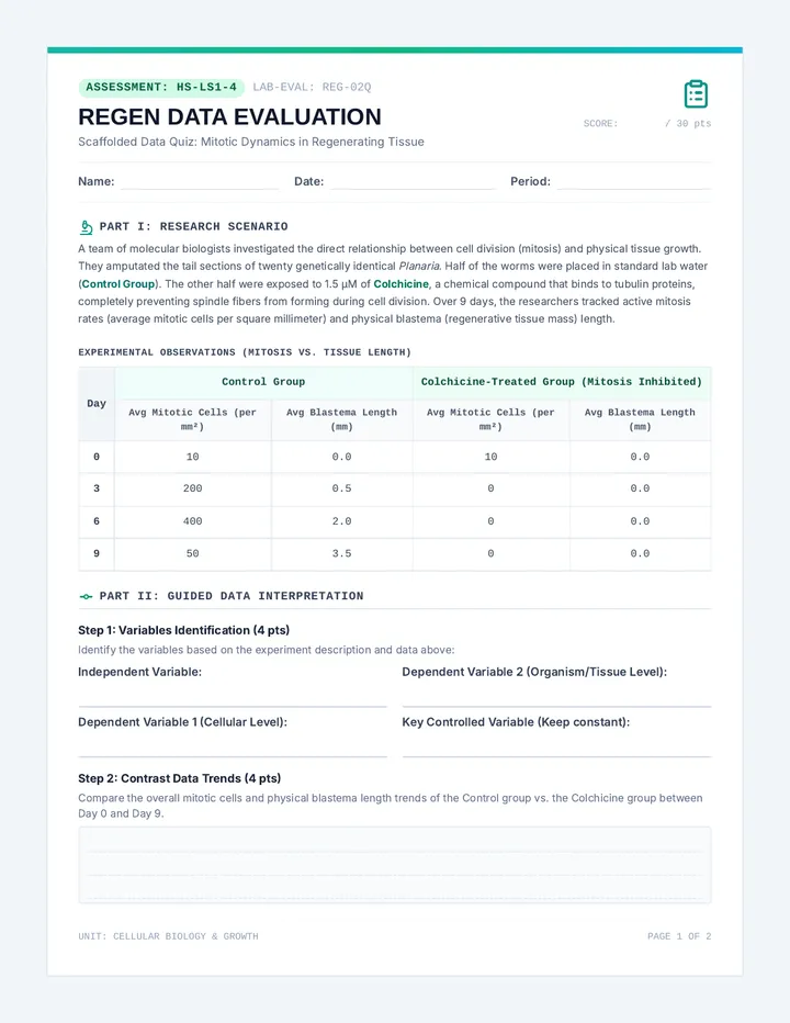
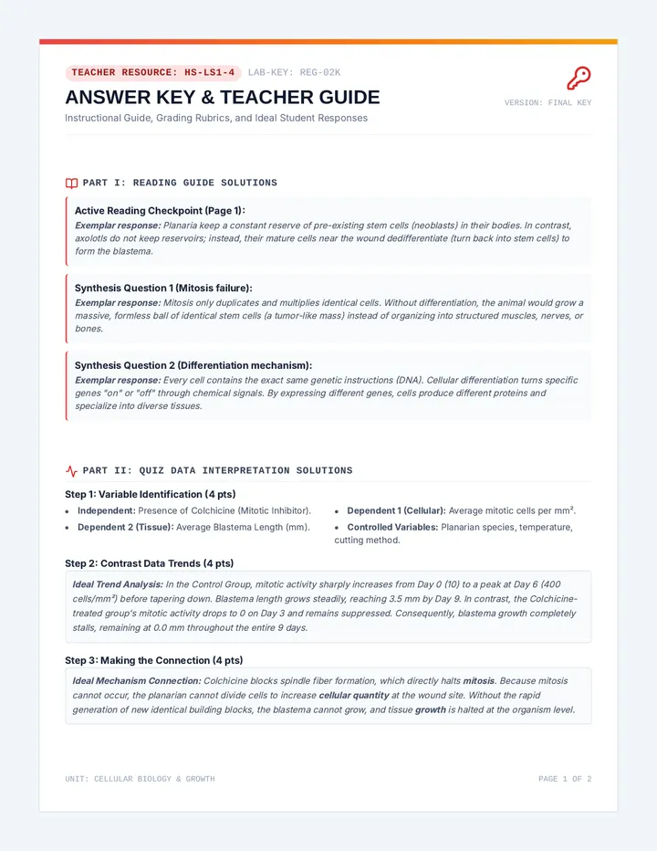
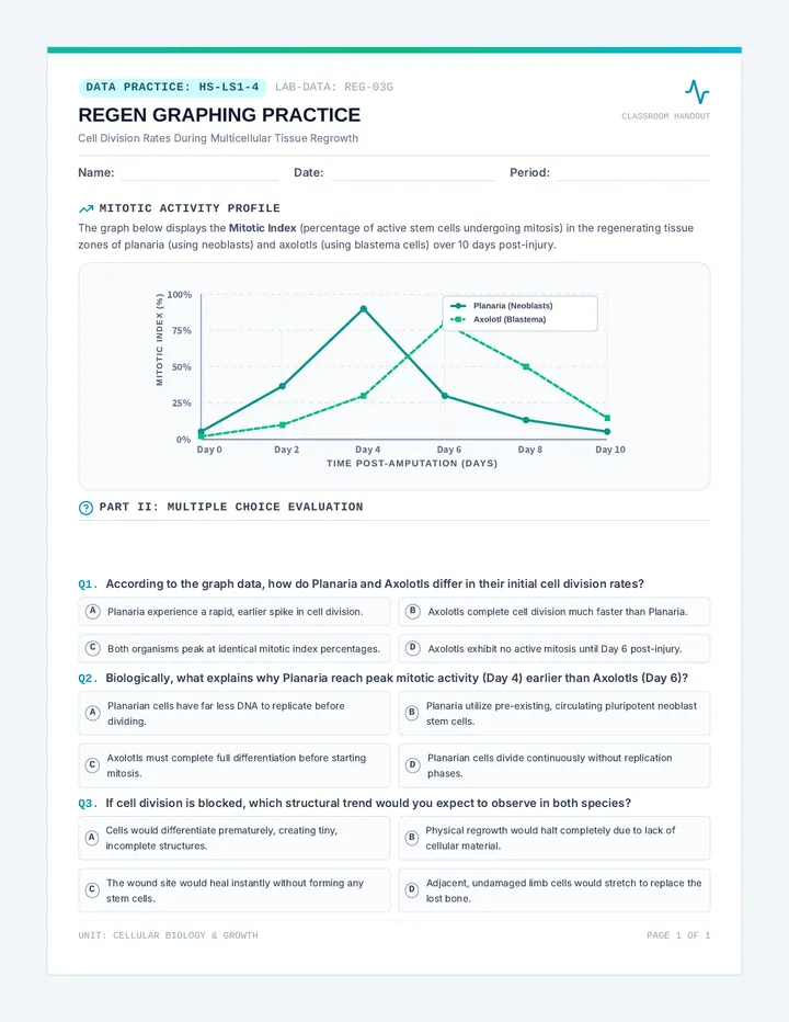
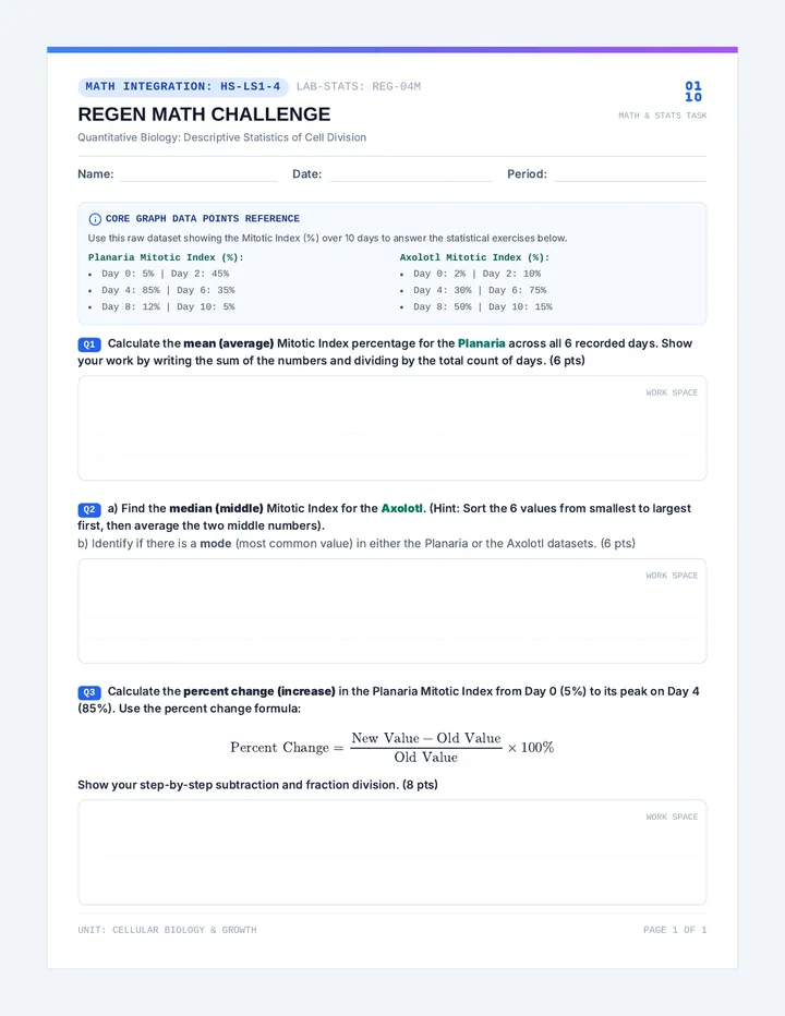
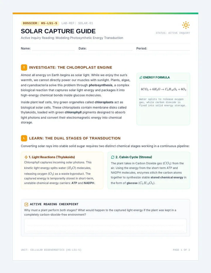
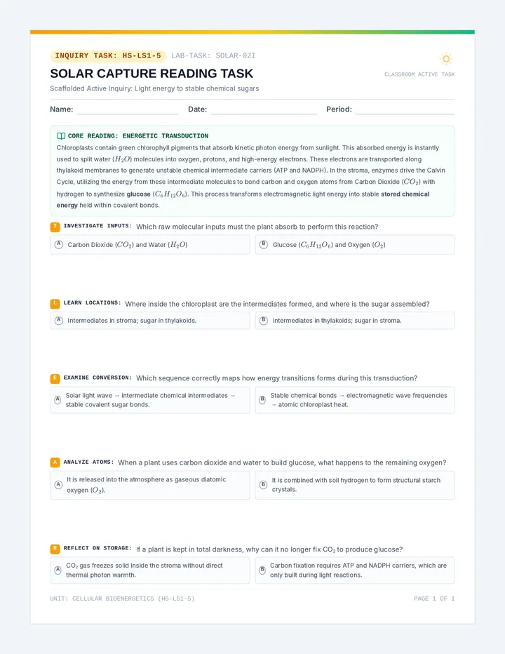
Orbital Overlap Slides Graduate Course: Solid State Chemistry
Tight Binding Transitions
From Molecular Orbitals to Periodic Band Structure
L1.01
The Power of \( N \)
Consider a diatomic molecule \( H_2 \). Two orbitals, two states: Bonding and Antibonding.
"What happens to the HOMO-LUMO gap when you connect \( 10^{23} \) atoms together?"
N=2
N=6
N \(\rightarrow \infty\)
Energy quantization transitions to a continuum.
Bloch's Theorem
In a periodic potential \( V(r + R) = V(r) \), the eigenfunctions of the Hamiltonian take the form:
\[ \psi_k(r) = e^{ik \cdot r} u_k(r) \]
\( u_k(r) \) has the same periodicity as the crystal lattice.
\( e^{ik \cdot r} \) is a plane-wave envelope factor.
The wavevector \( k \) defines the phase shift between unit cells.
Concept Check
Why is the magnitude of the wavefunction \( |\psi_k|^2 \) the same in every unit cell?
"The electron probability density must reflect the translational symmetry of the lattice."
k-Space (Reciprocal Space)
While real space describes positions \( r \), reciprocal space describes wavevectors \( k \).
Real Lattice
Periodicity \( a \)
Unit: Meters (m)
Reciprocal Lattice
Periodicity \( 2\pi/a \)
Unit: Inverse length (m\(^{-1}\))
The First Brillouin Zone (1st BZ)
The primitive cell in reciprocal space. For 1D: \( -\pi/a \le k \le \pi/a \).
0
+\(\pi/a\)
-\(\pi/a\)
k=0 (Gamma point)
Energy E(k)
The Tight Binding Result
For a 1D chain of s-orbitals with site energy \( \alpha \) and hopping integral \( \beta \), the band energy is:
\[ E(k) = \alpha + 2\beta \cos(ka) \]
\( \alpha \)
Site Energy
Atomic orbital energy
\( \beta \)
Hopping Integral
Overlap / Interaction strength
\( 4\beta \)
Bandwidth
Total energy range of the band
Key Takeaways
01
Orbitals overlap in solids to form continuous bands of allowed energy states.
02
Bloch's Theorem allows us to solve the Schrödinger equation for a periodic system using \( k \).
03
The dispersion relation \( E(k) \) connects electronic energy to the crystal's periodic lattice.
Up Next:
"How do we represent these bands for real materials? We'll dive into Band Structure diagrams and Density of States (DOS) to classify metals and insulators."
Go to Lesson 2
Bloch Functions Worksheet Bloch Functions Worksheet
Lesson 1: Tight Binding Transitions | Graduate Level
Student Name:
Date:
P1
The Periodic Potential
State Bloch's Theorem and explain the physical significance of the two terms in the expression \( \psi_k(r) = u_k(r) e^{ik \cdot r} \). Why must \( u_k(r) \) share the periodicity of the lattice \( a \)?
P2
Tight-Binding for a Homonuclear 1D Chain
Consider a 1D chain of identical atoms with spacing \( a \). We assume a single atomic orbital \( \phi \) per site. The crystal wavefunction is a Linear Combination of Atomic Orbitals (LCAO) satisfying the Bloch condition: \[ \Psi_k = \frac{1}{\sqrt{N}} \sum_{n} e^{ikna} \phi(r - na) \]
A) Show that \( \Psi_k(r + a) = e^{ika}\Psi_k(r) \). (Provide derivation steps below)
B) Using the Hamiltonian \( H \), the energy is given by \( E(k) = \frac{\langle \Psi_k | H | \Psi_k \rangle}{\langle \Psi_k | \Psi_k \rangle} \). If we only consider nearest-neighbor interactions, define the Coulomb integral \( \alpha \) and the Resonance integral \( \beta \). How does \( \beta \) relate to the orbital overlap?
P3
Visualizing the Band Structure
The resulting dispersion relation for the s-band is \( E(k) = \alpha + 2\beta \cos(ka) \).
1. Sketch the dispersion relation \( E(k) \) in the first Brillouin zone \( [-\pi/a, \pi/a] \). Assume \( \beta < 0 \) (typical for bonding overlap).
2. Label the following points:
\( k = 0 \) (\( \Gamma \) point)
\( k = \pm \pi/a \) (Brillouin zone boundary)
Energy at the center, top, and bottom of the band.
DRAW DISPERSION PLOT HERE
C) Physical Interpretation Questions:
i. Effective Mass
How does the width of the band (\( 4|\beta| \)) relate to the effective mass \( m^* \) of the electron at the bottom of the band?
ii. Nodal Structure
What is the physical reason for the energy being highest at \( k = \pi/a \)? (Hint: Consider the phase relationship between adjacent atoms).
EXT
Extension: Beyond 1D
If this were a 2D square lattice with lattice constant \( a \), what would the analytical expression for \( E(k_x, k_y) \) look like under the same nearest-neighbor approximations?
© 2026 QUANTUM CRYSTALS SERIES L1-WS01: BLOCH FUNCTIONS CONFIDENTIAL RESEARCH MATERIAL
Spaghetti Plot Slides Graduate Course: Solid State Chemistry
Spaghetti Plot Slides
Interpreting Band Structures and Density of States
L2.01
Complex Band Structures
Real crystals aren't 1D. We have multiple bands and complex symmetry directions in 3D k-space.
Key Features to Identify:
Fermi Level (\( E_F \)): The highest occupied energy at 0K.
Band Dispersion: Slope of \( E(k) \) curves.
Direct vs Indirect Gap: K-point of VBM vs CBM.
L Γ X W K L
Energy
"Reading the Spaghetti": E vs k across symmetry lines.
Density of States (DOS)
Number of States / Energy
Energy \( g(E) \)
DOS \( g(E) \) represents the number of states available at a given energy.
"Flat bands in k-space produce huge peaks in DOS. Dispersive (steep) bands produce low DOS."
Mathematically: \( g(E) \propto \oint \frac{dS_k}{|\nabla_k E(k)|} \)
Where the gradient of energy in k-space is the electron velocity .
The Fermi Level Rule
Metal
Fermi level passes through a band. Continuous states for conduction.
\( E_F \)
\( g(E_F) > 0 \)
Insulator
Fermi level in a large gap. No nearby states for conduction.
Large Gap (\( > 4 \) eV)
Semiconductor
Fermi level in a small gap. Thermally accessible states.
Small Gap (\( < 2 \) eV)
Silicon vs. Diamond
Silicon (Si)
Indirect band gap of 1.1 eV.
VBM at \( \Gamma \), CBM along \( \Delta \) (near X).
Requires phonon assistance for light absorption.
Diamond (C)
Wide band gap of 5.5 eV.
Transparent to visible light.
Excellent thermal conductor, electrical insulator.
DOS Analysis Worksheet DOS Analysis Worksheet
Lesson 2: Band Diagrams and DOS Analysis | Graduate Level
Student Name:
P1
The Gradient Connection
The Density of States \( g(E) \) is inversely proportional to the gradient of the energy in k-space: \( g(E) \propto \oint \frac{1}{|\nabla_k E(k)|} dS_k \).
A) Dispersion vs. DOS
Below are two generic dispersion curves. Sketch the corresponding DOS for each and explain the result in terms of the gradient.
Energy k
Sketch DOS
Energy
Sketch DOS
Explanation of physical difference:
P2
Van Hove Singularities
In 1D and 2D systems, the DOS often exhibits sharp peaks known as Van Hove singularities.
Identify the point in a 1D band \( E(k) = \alpha + 2\beta \cos(ka) \) where the DOS goes to infinity. What is the physical significance of this point in k-space?
How do these singularities typically differ between a 1D chain (nanowire) and a 3D bulk material? (Hint: Think about dimensionality and integration).
P3
Material Classification
Match the following DOS plots to their classification: Metal , Semimetal , Semiconductor , or Insulator . The dashed line represents the Fermi level \( E_F \).
L2-WS01: DOS ANALYSIS QUANTUM CRYSTALS SERIES
DOS Analysis Key DOS Analysis Key
Instructor Answer Key | Lesson 2
RELEASE: ACADEMIC YEAR 2026
FOR INSTRUCTOR USE ONLY
1
The Gradient Connection
Expected Sketch
Low slope:
\( \rightarrow \) High DOS
High slope:
\( \rightarrow \) Low DOS
Model Explanation
"The DOS counts the number of states per unit energy. When the energy band is flat (low gradient), a small change in energy corresponds to a large region of k-space, meaning many states share nearly the same energy. Conversely, a steep band means states are spread out over a large energy range, leading to a low density of states."
2
Van Hove Singularities
Identify the point:
The gradient vanishes at the Brillouin Zone boundaries (\( k = \pm \pi/a \)) and the center (\( k = 0 \)). At these points, \( \sin(ka) = 0 \), making the gradient zero and the DOS singular (\( \infty \)) in 1D.
Dimensionality Differences:
In 1D, DOS has \( E^{-1/2} \) singularities (peaks go to infinity). In 2D, they are logarithmic. In 3D, the DOS remains finite but has a "kink" or a vertical tangent. The more 'space' (dimensions) available to integrate over, the more the singularity is smoothed out.
3
Material Classification
A
METAL
States available at \( E_F \)
B
SEMIMETAL
Bands cross with zero/tiny DOS
C
INSULATOR
Wide energy gap
D
SEMICONDUCTOR
Small energy gap
Lattice Instability Slides Graduate Course: Solid State Chemistry
Peierls Distortion
Lattice Instability and the Metal-Insulator Transition
L3.01
Spontaneous Symmetry Breaking
"Why do perfectly conducting linear chains sometimes spontaneously turn into insulators at low temperatures?"
Nature seeks the lowest energy state. In 1D, a uniform metal is often unstable toward a distorted insulating state.
Uniform: Metallic
Peierls Distorted: Insulator
The Energy Trade-off
Distorting the lattice costs **Elastic Energy** but lowers **Electronic Energy**.
\[ \Delta E_{total} = \Delta E_{elastic} + \Delta E_{electronic} \]
Elastic cost: \( \propto \delta^2 \) (Stretching bonds)
Electronic gain: \( \propto \delta^2 \ln \delta \) (Opening a gap)
For small distortions \( \delta \), the logarithmic gain always wins in 1D!
Electronic Energy Lowering
Ef Gap opens at kF
Polyacetylene: The 1D Prototype
In polyacetylene \( (CH)_n \), if all C-C bonds were equal, it would be a 1D metal.
The Reality:
Bond-length alternation (Single-Double) opens a gap of ~1.5 eV. It behaves as a semiconductor/insulator.
Single Double Single Double
Charge Density Waves (CDW)
The lattice distortion is accompanied by a periodic modulation of the electron density.
Mechanism:
Electrons "pile up" in the shorter, stronger bonds and deplete in the longer ones. The period of the wave is \( \lambda = 2\pi/2k_F \).
Electronic Density Modulation
Distortion Dynamics Worksheet Distortion Dynamics Worksheet
Lesson 3: Peierls Distortion | Graduate Level
Researcher:
P1
The 1D Instability Criterion
Prove that a half-filled 1D band is always unstable to a doubling of the unit cell (Peierls distortion).
A) Reciprocal Space Folding
If the original lattice has constant \( a \), doubling the unit cell creates a lattice with constant \( 2a \). What happens to the First Brillouin Zone? Show that the original Fermi level \( k_F \) for a half-filled band now lies exactly at the new BZ boundary.
B) Energy Lowering Derivation
Why does opening a gap at the Fermi level always lower the total electronic energy of the occupied states, even if the conduction states are pushed up?
P2
Molecular vs. Solid State
The Jahn-Teller Effect in discrete molecules is often described as the local counterpart to the Peierls Distortion .
Compare these two effects. How does the "electronic state" in a molecule (e.g., degenerate orbitals) relate to the "electronic state" in a 1D metal (e.g., the Fermi surface)?
Thought Experiment
"If we increased the dimensionality to 3D, why does the Peierls distortion typically disappear or become much weaker? (Think about the 'perfect nesting' of the Fermi surface)."
P3
Case Study: Polyacetylene
Trans-polyacetylene has two degenerate ground states (Phase A and Phase B). A domain wall between these two phases is known as a soliton .
Draw a schematic of a soliton in a polyacetylene chain, highlighting the non-bonding electron.
SOLITON SCHEMATIC
How does the presence of solitons affect the conductivity of doped polyacetylene?
L3-WS01: DISTORTION DYNAMICS QUANTUM CRYSTALS SERIES RESEARCH CLASSIFIED
Doping Dynamics Slides Graduate Course: Solid State Chemistry
Doping Dynamics
Fermi Level Engineering in Semiconductors
L4.01
Impurity Power
"How does introducing a few impurity atoms per million transform a useless crystal into the backbone of the computer age?"
Intrinsic semiconductors are insulators at low T. Doping introduces local states that shift the Fermi level, creating charge carriers (electrons or holes) that move through the band.
P
Substitutional Doping (n-type)
Fermi Level Shifting
n-type (Donor)
Group 15 (e.g., P) in Si. Donor states lie just below the conduction band.
EF
Fermi level shifts UP toward CBM.
p-type (Acceptor)
Group 13 (e.g., B) in Si. Acceptor states lie just above the valence band.
EF
Fermi level shifts DOWN toward VBM.
The p-n Junction
When p-type and n-type materials contact, the Fermi levels must align at equilibrium.
Consequence: Band Bending
Internal electric fields are created, forming a **depletion region** that acts as a barrier to charge flow.
EF p-side n-side
Band Gap Engineering
By creating alloys (heterojunctions), we can continuously tune the band gap.
"For Al\(_{x}\)Ga\(_{1-x}\)As, the band gap varies linearly with \( x \). This allows for precisely tuned LEDs and Lasers."
Tuning Optical Properties
1.4 eV
1.8 eV
2.4 eV
3.2 eV
Small Gap Large Gap
Junction Engineering Worksheet Junction Engineering Worksheet
Lesson 4: Semiconductors and Doping | Graduate Level
Project Lead:
P1
Carrier Concentrations
The intrinsic carrier concentration \( n_i \) is given by \( n_i^2 = n \cdot p = N_c N_v e^{-E_g/kT} \).
A) n-type Doping Calculation
If Silicon (\( E_g = 1.1 \text{ eV} \)) is doped with \( 10^{17} \text{ cm}^{-3} \) Phosphorus atoms, calculate the hole concentration \( p \) at room temperature (300K). Assume \( n_i \approx 10^{10} \text{ cm}^{-3} \).
Conceptual Check:
"Does doping Silicon with Phosphorus change the value of \( n_i \)? Why or why not?"
P2
Heterojunction Band Alignment
Consider a heterojunction between two semiconductors, Material A and Material B. Material A has a larger band gap than Material B.
Sketch a Type-I (Straddling) band alignment and a Type-II (Staggered) band alignment. Indicate where electrons and holes would accumulate in each case at equilibrium.
SKETCH ALIGNMENTS HERE
B) Application in Optoelectronics:
Which alignment (Type-I or Type-II) is generally preferred for a high-efficiency LED? Explain your reasoning in terms of charge carrier recombination.
P3
Depletion and Bias
Explain what happens to the width of the depletion region in a p-n junction under forward bias vs. reverse bias . How does this dictate the "rectifying" behavior of a diode?
L4-WS01: JUNCTION ENGINEERING QUANTUM CRYSTALS SERIES FOR ADVANCED RESEARCH ONLY
Crystal Imperfection Slides Graduate Course: Solid State Chemistry
Crystal Imperfections
Defects, Non-Stoichiometry, and Color Centers
L5.01
The Beauty of Brokenness
"Why are rubies red and sapphires blue when they are both made of the same aluminum oxide crystal?"
Perfect crystals don't exist in nature—and if they did, they'd be boring. Defects introduce new energy levels in the band gap, enabling color, magnetism, and ionic conductivity.
Ruby
Cr\(^{3+}\) in Al\(_2\)O\(_3\)
Sapphire
Fe\(^{2+}\)/Ti\(^{4+}\) in Al\(_2\)O\(_3\)
Point Defects
Schottky Defect
Paired vacancies of anions and cations. Maintains charge neutrality and stoichiometry.
Common in highly ionic crystals (NaCl, KCl).
Frenkel Defect
An ion leaves its lattice site and moves into an interstitial position. No change in density.
Common in AgCl, AgBr.
F-Centers (Farbe Centers)
An F-center is an **anion vacancy** occupied by one or more electrons.
Electronic Trap
The trapped electron acts like a "particle in a box," with quantized energy levels that can absorb visible light.
• Heating NaCl in Na vapor creates yellow color.
• Heating KCl in K vapor creates violet color.
e-
Non-Stoichiometric Compounds
Transition metal oxides often deviate from perfect integer ratios.
Example: Fe\(_{1-x}\)O
Wüstite (FeO) is never Fe\(_{1.0}\)O. It is usually Fe\(_{0.95}\)O.
Charge is balanced by oxidizing some Fe\(^{2+}\) to Fe\(^{3+}\), turning the material into a p-type semiconductor.
Emergent Properties
High ionic conductivity (Battery tech)
Complex magnetic ordering
Enhanced catalytic activity
Defect Detective Worksheet Defect Detective Worksheet
Lesson 5: Defects and Deviations | Graduate Level
Investigator:
P1
Why Defects are Inevitable
The equilibrium concentration of vacancies \( n \) in a crystal of \( N \) sites is given by \( n/N \approx e^{-\Delta H_v / kT} \).
A) Briefly explain why the Gibbs Free Energy \( G = H - TS \) is minimized when a certain number of defects are present, even though creating a defect always costs enthalpy (\( \Delta H_v > 0 \)).
B) If the enthalpy of vacancy formation in a metal is 1.0 eV, calculate the fraction of vacant sites at 300K vs. 1000K. What does this imply about the temperature dependence of solid-state diffusion?
P2
Kröger-Vink Exercises
Write the defect reactions for the following processes using Kröger-Vink notation:
1. Schottky defect in NaCl:
2. Frenkel defect in AgBr:
3. Incorporation of CaCl\(_2\) into NaCl:
Recall: V for vacancy, ' for negative charge, • for positive charge, x for neutral.
P3
Property Prediction
Case A: Ionic Conductivity
You have a sample of ZrO\(_2\). You dope it with Y\(_2\)O\(_3\) (Yttria-stabilized zirconia). How does this affect the oxygen ion conductivity? Write the relevant defect equation.
Case B: Color Centers
A transparent crystal of MgO is exposed to high-energy radiation, creating oxygen vacancies. The crystal turns blue. Explain the electronic origin of this color.
P4
The Wüstite Problem
In Fe\(_{0.95}\)O, determine the percentage of Iron atoms that must be in the \( 3+ \) oxidation state to maintain charge neutrality. Assume all oxygen is \( O^{2-} \).
L5-WS01: DEFECT DETECTIVE QUANTUM CRYSTALS SERIES
Solid State Seminar Project Guide Solid State Seminar
Capstone Research Project | Band Theory & Bonding Sequence
Final Assessment
Project Objective
Working in pairs, you will select a "Modern Functional Material" and perform a deep-dive analysis of its electronic structure. Your goal is to explain how its specific bonding and band structure give rise to its unique macroscopic properties. You will present your findings in a 10-minute seminar format.
Deliverables
1. Band Structure Report
A 3-page technical report featuring a literature-sourced band structure diagram and DOS plot. You must label the Fermi level and identify the character of the bands (e.g., O-2p valence, Ti-3d conduction).
2. Oral Seminar
A visual presentation (slides) highlighting the "Structure-Property" relationship. How does the chemistry of the atoms dictate the band gap or conductivity?
Suggested Topics
Perovskite Solar Cells (MAPbI\(_3\))
Direct vs. Indirect gaps and spin-orbit coupling.
Graphene & 2D Materials
Dirac cones and zero-gap semiconductors.
Topological Insulators (Bi\(_2\)Se\(_3\))
Bulk band gap vs. conducting surface states.
TMDs (MoS\(_2\))
Indirect-to-direct gap transitions in monolayers.
Assessment Rubric
Criterion Exemplary (5) Proficient (3) Emerging (1) Band Analysis Correct identification of orbital contributions and k-point symmetry. General description of bands provided with minor errors. Inaccurate labeling or fundamental misunderstanding of DOS. Concept Synthesis Seamlessly links Bloch's theorem to physical properties (e.g. effective mass). Identifies connections but lacks mathematical rigor or depth. Lists properties without connecting to band theory. Clarity & Presentation Professional visuals; clear, high-level scientific communication. Effective communication; some visual clutter or pacing issues. Difficulty explaining concepts; poor visual quality.
Project Timeline: 3 Weeks total (Research, Analysis, Seminar)
REF: QUANTUM-FINAL-P01